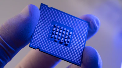
Heat traps buried deep within vertically stacked 3D heterogeneous integration (3DHI) packages escape detection in surface-level thermal scans, and engineers may discover them only after a chiplet fails. Reliable 3D chip thermal management starts with subsurface thermal mapping that precisely shows where heat accumulates within each tier of the stack. Transient thermoreflectance imaging delivers that map and tells engineers how to adjust materials and layer placement before failure.
The Hidden Limits of Traditional 3D Chip Thermal Management
Conventional infrared thermography works well on flat, single-layer dies because thermal radiation travels a relatively unobstructed path from the heat source to the camera, unlike in heterogeneous packages that contain diverse and dynamic layers of chips. Stacked 3DHI packages break that path with bonding layers and additional silicon dies above any buried hot spot.
A surface-level scan can miss those hot spots entirely, causing a next-generation dense chiplet package to clear review while its hottest interface lies several tiers down. The problem then appears only as premature failure in the field.
How Transient Thermoreflectance Pinpoints Buried Heat Traps
Because silicon transmits near-infrared light, a transient thermoreflectance imaging (TTI) system can scan through active tiers to reach buried layers. The time-resolved thermal wave propagation it records adds depth information, since the timing of each thermal response reads as a clock that helps estimate a bottleneck's depth and location before heat spreads across the package.
Time-domain thermoreflectance (TDTR), a pump-probe technique, can measure thermal conductance across material interfaces along with thermal conductivity tensors. It also yields the volumetric heat capacity of thin films, bulk materials and 2D materials. Its ability to resolve thermal properties spatially helps in studying heterogeneous material systems.
According to the National Institute of Standards and Technology (NIST), transient thermoreflectance techniques achieve a spatial resolution below about 1 micron at the fine end and roughly 10 microns at the coarse end, depending on the optics. They probe depths from approximately 50 nanometers to 1 millimeter and measure thermal conductivity from roughly 0.1 W/mK to more than 500 W/mK, with some techniques exceeding 2,000 W/mK.
Sub-Micron Bottlenecks in Hybrid Bonding and Thermal Boundary Resistance
Below 10 nanometers, thermal boundary resistance (TBR) ranks among the biggest obstacles to heat flow in advanced logic chips. TBR is the resistance that heat encounters when it crosses from one material to another.
Porous low-k SiCOH, an insulating film that surrounds copper wiring in the chip's upper wiring layers, adds a separate obstacle. It conducts heat at only 0.1 to 0.5 W/mK, less than one-tenth of the conductivity these densely packed layers need to carry heat away.
Ultra-low-k formulations perform worse still, since the air gaps that lower their dielectric constant leave almost no pathway for heat conduction. Once interconnect lines narrow below 20 nanometers and carry heavier current, tiny flaws in the insulating material around them can trap heat. Pores, voids, seams and weakly bonded interfaces each slow the route that heat takes out of nearby transistors and wiring.
According to a review of 2.5D and 3D chiplet integration by University of Florida scientists, microbumps and hybrid-bond interfaces add boundary resistance and heat the stack unevenly. Published measurements of hybrid-bonded memory stacks show roughly tenfold the junction-to-case thermal resistance in advanced 2.5D modules. Interconnect pitches nearing single-digit microns in Intel Foveros and TSMC 3D-SoIC lengthen the heat-extraction path further.
Engineers can measure how readily heat crosses each interface and how well each layer conducts it, then feed those values into thermal modeling software. Simulations built on measured values tend to place hot spots closer to where they form in the real stack. When a void or weak bond builds resistance at one interface, the model can carry that higher value and show how it shifts temperatures nearby.
The Role of Inspection and Metrology in Thermal Reliability
Common semiconductor inspection applications include defect inspection and critical dimension (CD) metrology, among others. Optical or e-beam systems scan for particles, scratches and pattern defects, while CD tools measure features such as lines and vias with sub-nanometer precision.
Each chip can hold billions of transistors across layers of components that grow more intricate as features shrink. Today's inspection tools need nanometer precision, since one defect can cause an entire device to fail. A buried void in a dense 3DHI package may trap enough heat to cause a similar outcome.
Interface Materials That Prevent Thermal Failure
Tantalum-based liners and titanium nitride barriers help suppress diffusion and electromigration in copper wiring, yet both impede heat dissipation from the metal they protect. Even at a few nanometers thick, these layers add measurable TBR. Comparing that value across candidate liners may show design teams how much heat flow each diffusion barrier costs.
Indium phosphide is a raw material for semiconductor chips, and its direct bandgap and low current density, together with high collector and large-emitter capacitance, have made it popular in microelectronics. Because those traits are electrical, designers still need thermal measurements at the bonded interface to judge how a candidate material conducts heat.
How Thermal Modeling Data Guides Layer Placement
In dense chiplet packages such as 3D integrated circuits and 2.5D interposers, localized heat fluxes and vertical stacking create extreme thermal dissipation challenges. In fully 3D stacks, thermal coupling between neighboring dies also promotes correlated hot spots.
Per the previously mentioned University of Florida research, air cooling remains viable for 2.5D stacks at roughly 300 watts. 3D stacks need liquid or hybrid cooling along with high-performance interface materials at about 350 watts.
The same study singles out interposer conductivity and thermal interface material thickness, along with hot spot power distribution, as the inputs that sway 3D chip thermal management results most. A silicon interposer in a 2.5D package conducts heat along its plane at about 150 W/mK, but the underfills and dielectric layers around it have significantly lower cross-plane thermal conductivity, a directional gap that engineers call anisotropy.
Tests and models of high-density 2.5D packages show that interposer hot spots can exceed 120° Celsius when total power exceeds 600 to 700 watts. Engineers may use imaging data to map hot spots and locate structural defects, then focus on the thermal resistance that most needs optimizing. Depth-resolved maps also provide a measured basis for layer placement decisions, so design teams can compare alternative tier orders and interface materials against the map and rescan each revision.
Thermal Maps Replace Guesswork in Chiplet Reliability
Subsurface thermal mapping provides engineers with sufficient evidence at the stage when a stack is easiest to revise. Teams that adopt it early may move thermal analysis from post-failure troubleshooting into the first architecture decisions, when a thermal map can still reshape the design.