Mechanical tolerance issues can wreak havoc on manufacturing your integrated microelectronic medical device, adding unnecessary costs and delays throughout the product development process and negatively impacting final functional yield.
Discovering problems caused by mechanical tolerances at the production stage is very expensive due to the need to change and source multiple components, update manufacturing processes, and repeat or redesign verification and/or validation activities or conduct risk assessments associated with limiting scope of retesting.
It's absolutely critical to determine when materials and processes simply don't stack up by investing in careful study of assembly margins and process capability in a stepwise fashion, and it's important to pay close attention to the compatibility of everything involved in developing your medical device, at a time when things can be planned and adjusted — during the design stage.
What causes mechanical intolerances?
The root causes of many tolerance issues typically start at the top. Most medical device designers take a "top-down" approach to determining what is needed to make a product work. After all, top-level function is most visible and ultimately validated before product release. While this may sound intuitive, this outside-in view is counter to how the tolerances of all the parts involved in your device should be considered — from the bottom up. Knowing which lower-level requirements must be properly understood and managed to ensure top-level function is paramount to proper design.
Adding to this complexity, accommodating the intrinsic design variation of every component within the system is only half the process; the manufacturing processes used to assemble these components generate another source of variation. How you build is as important as what you build. Uncovering these "hidden requirements" is a complex process.
Each part within a design carries its own tolerance and has unique characteristics that manifest when exposed to process constituents within the entire system. They will function well together – or not – depending on how they are stacked upon each other.
For the complex design that today's modern devices require, start with an estimating process for tolerances, which can be difficult to assess accurately because each part is impacted by the other parts' mechanical tolerances when they are joined and function together.
However, a modern computer-aided design (CAD) package effectively simulates variation in the final stack and provides reasonable design inputs. Off-the-shelf (OTS) components have dimensional tolerances specified on their drawings. For custom parts, consider typical tolerances consistent with their method of manufacture. Fabricate a reasonable sample of mission-critical components and measure their as-made variation.
The materials, tools, and processes used during assembly further complicate the mix, given they also alter the tolerances within the design and thus can compromise functionality and decrease yield of the end product. Collaborate with the manufacturing engineers to understand typical variation of assembly processes under consideration.
If the top-level tolerance requirements are close to the first-level tolerance stack-up approximation, best practice dictates a test build and careful measurements of representative parts to tease out the ultimate stack tolerance and which parts and processes carry the highest risks. This is easiest to derive from the bottom up when fewer parts and processes are stacked, and direct measurement is simplest, though this is not how most device designers think. Yet, as devices become smaller and more integrated, this is a requisite for ultimate success.
New approaches
In the "old days" of medical device design – about five to 10 years ago – products were not as integrated as they are today. Many products were an integration of OTS subassemblies that are "known good" assembled with standard processes. Development cycles of the past consisted of building a small number of prototypes, testing to see if everything worked at higher levels, and moving to the production stage -- building the assembly line after design and specifically for the number of devices to be manufactured.
This approach doesn't work when developing today's highly integrated devices when each element and subassembly must be scrutinized. Intricate tolerances among multiple parts, materials, and assembly processes must align for compatibility and repeatability. The higher the number of varying components and assembly steps, the bigger the risk of tolerance problems.
Today, the design of the product and the design of the production line for that product should happen simultaneously, with each level of integration considered one step at a time. Start from the beginning (the bottom), thoughtfully design your parts/materials/processes, build a population, and measure/test. Measure each part's dimensional variation at the base level. Each build should be leveraged as a small-scale run through the manufacturing process – use intended final toolsets and gradually refine build documentation and in-process quality measurements/checks.
Next, adding one part to another, continue to measure and test the combined tolerance and subsystem performance, if appropriate. Ask yourself, "What do you see?" (reality) and compare it to "What do I expect to see?" (your plan) for all parts within the population. Does subsystem performance break down when a measurable tolerance is exceeded? If not, perhaps the tolerance can be expanded to save cost or to simplify/expand sourcing options; over-specification can also have negative consequences!
This collaborative learning creates your basis of "hidden requirements" for all teams and product and manufacturing designs while also developing (sub)system testing and the product supply chain. Once appropriately understood, proceed to the next step of integration. If not, make changes to the design and/or assembly process/materials until there is understanding, and then move ahead. If you are unsure whether the design is robust enough at a lower integration level, intentionally build and carefully label a larger population of parts at or beyond each end of the stack-up range to be integrated and tested at the next level.
Often, new hidden requirements are uncovered, highlighting critical design problems that were unknown before test build characterization – this is like gold for the product development team. Often, these learnings are associated with the impact of a process used for assembly.
Consider the common case of attaching a printed circuit board (PCB) to a mechanical component using adhesives. The PCB has multiple lateral and vertical tolerances, varying with the thickness and flatness of the board and alignment of mounting holes, traces, and other features. Processing the adhesive often adds additional curvature to the system that far exceeds the other mechanical tolerances of the adjoined components. This warpage is resultant from the mismatch of the coefficient of thermal expansion (CTE) between materials within the stack and elevated temperatures used to cure the adhesive.
Countermeasures to this warpage may include:
- Changing the adhesive stiffness
- Changing adhesive dispense locations and/or bondline thickness
- Changing adhesive curing conditions
- Selecting an adhesive that cures at lower temperatures or via another mechanism – such as UV light exposure
- Matching the CTE of the materials being adjoined by changing their base materials
- Changing the mechanical stiffness of the PCB material
- Changing other processing/handling steps associated with adhesive dispense and cure.
Changes, even subtle changes, can have a massive impact on product performance, cost, and yield.
Taking this approach can reveal important considerations well before the device's final design is complete. Because you're building from the bottom up, integrating one part with material at a time, you can identify manufacturing steps that may alter tolerances, and you'll have a clearer view of where current and future problems may occur, allowing you to identify critical issues and iterate on solutions to resolve them.
Investing the time and money in this stepwise integration saves in the long-term by reducing scrap and costly rework commonly encountered upon production ramping when the real product distributions are observed for the first time. In the worst-case scenario, the product yield is so low that a total redesign is necessary.
A Recent Case Study
An OEM device company needed to place a sensor onto a round substrate within a 50-micron tolerance referenced to the center of the circle in the X- and Y-axes to enable functionality. While this requirement seemed simple and straightforward to build with machines having a 10-micron placement accuracy, it became challenging because the substrate had certain features that add error to the system. Careful metrology of a population of substrates to be assembled showed that critical substrate features were patterned with 25-micron tolerance.
Further, the substrates were laser singulated from a panel, adding another 25-micron tolerance. Stacking these tolerances would exceed the 50-micron error budget within the material and build processes and highlight a critical issue impacting build yield. Something needed to change to achieve an acceptable production yield.
Adjustments were made to the method of fabricating the incoming material to reduce dimensional variation. Though this material increased cost, the total product cost was reduced through improved processing yield. We also adjusted the assembly processes to reference different datums within the system to further close the gaps and ensure success. By keeping builds small and investing in making careful measurements and understanding their impact on the product stack, the team was able to improve yield from 30 percent to greater than 90 percent.
The devil in this device's details were hidden at the deepest levels of design. Here, we summarize how to reveal and fix mechanical tolerance stack-up problems by taking a bottoms-up view:
Prototyping
Keep your prototype builds as simple as possible. Instead of integrating the entire product stack in a single build, start with the first build step, measure its output, and learn what worked and what did not. Use the anticipated manufacturing tools and process of record for each step. When needed, adjust the design, tools, and/or processes to solve these issues and repeat the measurements to verify that you were successful. Once a "known good" stack is in hand, add the next level of integration and repeat the process again.
When assessing the impact of variation, sample size matters. Build and measure reasonable numbers to gain a sense of the variation within what is being produced; a build size of 20-30 units is a reasonable starting point to understand inherent population variation. If process variation is driving the stack-up variation, then multiple builds may be prudent to establish sufficient stability. Keeping the prototype builds simple also helps in saving costs. Often, lower cost "dummy" units are used to assess mechanical tolerances without requiring full functionality. Dummy units are also used to save time as they are often faster to source and update.
Don't hold back on the number of prototype builds. Instead of one or two build cycles of high complexity, plan to build five or even 35 iterations of simplified integrations. This is often the only way to get the data you need to make well-informed early design decisions. Taking multiple sets of measurements along the way helps identify where to spend early money when choosing the most compatible parts and materials that may be more mechanically favorable to the overall design and production of the device.
These dummy prototypes may never be functional; they are meant to build understanding of how varying tolerance combinations stack up for the long term. Even though the prototypes are experimental, take the time to develop real tests, assess various materials to be assembled, iterate real manufacturing processes and equipment, and develop appropriate metrology. This modern prototyping approach may require more up-front budget and time but saves critical time and money later in the product development cycle when the stakes are highest.
Investing early to save later
The use of certain materials during production can change the quality of your parts at higher levels of integration. For example, if your assembly process requires thermal curing adhesives, your bonded assembly's mechanical form will be subject to warpage resulting from the CTE mismatch between materials you are bonding. It is not uncommon that changing a PC board from an organic material to a higher-cost ceramic reduces the final product cost through improved yield due to lower CTE and higher mechanical stiffness afforded by ceramics. Parts may also move during curing, so care should be paid to design fixturing to properly retain parts while adhesives harden.
To assess the tradeoffs between input material costs and acceptable process yield, test builds with varying materials should be assembled and measured. In one instance, the outcome was an increase from 10 percent to 80 percent in yield just by making this change at the beginning. Realize that it's not necessarily the cost of the bill of materials that drives the end price of the product; it is the higher assembly costs and lower yields that come later. This is especially true for complex assemblies where the labor-add of manufacturing and yield loss can often far exceed the raw bill of materials cost.
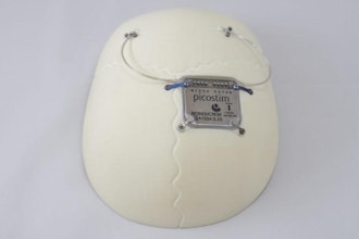
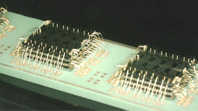
 A complex device requiring meticulous attention to the entire manufacturing process flow to prevent thermal stress breaks. The order of process steps becomes as important as the material selection in building these types of devices.Promex
Reorder your steps
Think through the order of operations required to produce your device. Considering CTEs, for example, may lead you to discover that bonding a surface to another surface may cause warpage. Yet, you may be able to add parts onto that surface in a way that allows them to act as 'stiffeners' and thus increase the mechanical stability of this sub-assembly. Discoveries like this can only be revealed when you experimentally reorder the steps in the design process and measure the output.
Adjust assembly tools
The tools used in the assembly process also have different mechanical strengths and weaknesses, which should be understood as you design the manufacturing cycle for your device. For example, using a tool for higher placement accuracy may seem unnecessary when you take a top-down view, yet from the bottom-up, you can see which assembly tool to choose for the assembly process within your design.
Another example is choosing tools that apply certain heat locally to parts in place rather than heating the entire device. This decision can improve the CTE mismatch effect.
Carefully crafting mechanical tolerances into both the device design and its manufacturing process, from the bottom up, tips traditional device development on its head. While this new mindset may require more time and money at the onset of a device project, it will pay off in the end, again and again, with a greater return from saved time and money throughout production and higher (and higher quality) yields.
If your current CDMO hasn't proposed this point of view and your devices are getting more complex, smaller, and integrated, it may be time to interview new partners. Choose one with expertise in the bottoms-up co-design of devices and their production processes, with a wide range of parts, materials, and tools on hand to try and test in the early stages. Together, you can make critical, prudent decisions that will affect the bottom line of your devices and your business.
Dave Fromm is chief operating officer and vice president of engineering at Promex, the market leader in microelectronic assembly for the medtech and biotechnology markets. Promex has the broadest set of manufacturing capabilities under one roof and an open-door collaborative new product development lab for medical device designers. With cutting-edge equipment, extensive material properties knowledge, and meticulous supply chain management, Promex partners with OEMs at all stages, from early prototypes to R&D development and high-volume production.


