Medical sensors have never been more capable. Advances in MEMS, optics, microfluidics, and semiconductor technologies have enabled devices that can detect smaller signals, monitor more parameters, and operate in increasingly compact form factors. From wearable health monitors and implantable sensors to lab-on-a-chip diagnostic platforms, today's devices are delivering clinical insights that were unimaginable just a decade ago.
Yet many sensor programs encounter an unexpected challenge as they move toward commercialization: performance that looked excellent in the lab becomes difficult to reproduce consistently in manufacturing.
The reason is simple. In many next-generation medical devices, sensor performance is no longer limited by the sensing technology itself. Instead, it is increasingly constrained by materials, assembly processes, packaging architectures, and manufacturing variability.
For device designers, understanding this shift is becoming critical to successful commercialization.
The Sensor Is No Longer a Standalone Component
Historically, sensors were often treated as discrete components integrated into a larger system. Today, they are more commonly embedded within highly integrated assemblies that combine microelectronics, optics, mechanics, fluidics, and chemistry.
This trend toward heterogeneous integration creates significant opportunities. Devices become smaller, more capable, and more power-efficient. At the same time, however, sensor performance becomes dependent on interactions throughout the entire assembly.
A highly sensitive optical sensor, for example, may be affected by adhesive shrinkage during cure. A MEMS structure may experience stress due to thermal expansion mismatches within the package. A biochemical sensor may degrade because of exposure to temperatures or environmental conditions encountered during manufacturing. In these systems, the sensor can no longer be evaluated in isolation.
With optical systems used in diagnostic devices, minor alignment errors measured in microns may be enough to reduce signal quality or introduce measurement variability. Similarly, MEMS structures may respond differently if assembly-induced stresses alter their geometry or operating conditions.
As devices become smaller, process windows shrink as well. Small variations in adhesive thickness, substrate flatness, or placement accuracy that were once inconsequential can now affect sensor output.
This shift changes manufacturing from simply building the device to actively preserving the performance designed into it.
Materials Are Now Performance-Critical Components
One of the most overlooked contributors to sensor performance is material selection.
Materials are often chosen based on their intended functional role: structural support, insulation, biocompatibility, thermal management, or optical transmission. However, their behavior during manufacturing can be equally important.
For example:
- Adhesives may shrink during cure and alter alignment.
- Substrates with mismatched coefficients of thermal expansion can introduce stress.
- Coatings may change optical properties after environmental exposure.
- Encapsulants may affect heat dissipation or long-term reliability.
These interactions become especially important in miniaturized devices where component spacing is measured in mils or even microns.
Designers increasingly must evaluate materials not as individual selections but as interconnected systems. Successful products often emerge from early collaboration between design and manufacturing teams that understand how material choices influence assembly outcomes.
A useful framework is to map each material in the assembly against three questions: How does it behave during processing (temperature, chemistry, mechanical stress)? How does it interact with adjacent materials over time? And does it introduce variability that will affect sensor output at the system level? In one class of sensor-integrated diagnostic device – flip-chip assemblies for particle physics detectors – traditional flux-based solder reflow had to be abandoned entirely because post-solder cleaning solvents damaged delicate detector surfaces. The solution was vacuum reflow using formic acid as a fluxless process, combined with precision fixtures whose coefficient of thermal expansion was matched to the bonded die and substrate. Neither choice was obvious from the component datasheet alone; both emerged from treating the material system as a whole.
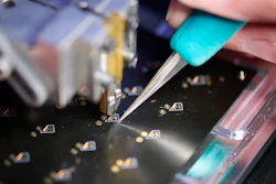
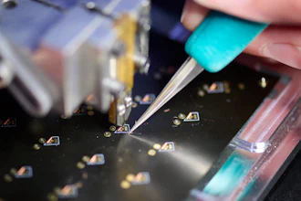
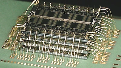
 Multi-die flip-chip assembly on substrate. At micron-scale tolerances, manufacturing process control is inseparable from sensor performance.Promex
The Challenge of "Invisible" Components
Some of the most difficult sensor assemblies involve components that are challenging to inspect, handle, or even see.
Examples include:
- Transparent optical elements
- Thin flex substrates
- Functionalized biochemical surfaces
- Microfluidic structures
- Submillimeter MEMS devices
Traditional automated assembly systems were not developed with many of these components in mind. Machine vision systems, for example, may struggle to detect transparent materials or low-contrast features.
As a result, manufacturers are increasingly developing customized workflows, fixturing strategies, and inspection methods specifically for these advanced components.
Consider, for example, a genomics consumable cartridge that integrates a silicon sensing die with pre-applied surface chemistry. The chemistry imposes assembly constraints unrelated to the sensor’s electrical performance: it cannot get wet, cannot be exposed to temperatures above 40°C, and is sensitive to light. Standard wafer dicing – which submerges the wafer in DI water – is immediately disqualifying. Wirebonding, which typically involves a heated stage, must be redesigned for near-room-temperature operation. Even the adhesive used for die attach must cure at low temperature, and outgassing during cure must not impact the device chemistry. In this type of device, the sensor’s performance specification is the easy part. The manufacturing process is where the design either succeeds or fails.
In many cases, success depends less on the sensor itself and more on the ability to reliably integrate delicate elements into a repeatable production process.
Practical approaches engineers can use when facing invisible-component or sensitive component challenges include: programming machine vision systems with illumination angles and contrast settings calibrated to the specific material (rather than relying on default setups); using protective release tape during wafer dicing to shield functionalized surfaces and prevent debris from reaching the active area; and developing adhesive dispense protocols tuned for low-viscosity optical adhesives that must flow without bubbles and maintain coplanarity between bonded surfaces. For a miniaturized multispectral fluorescence detection system requiring components within a 1 cm³ volume – including sapphire and quartz optical elements with delicate anti-reflective coatings – each of these techniques was required in combination, along with Class 100 cleanroom assembly and automated 3D pick-and-place that could locate and handle optically transparent parts.
Yield Loss Often Reveals Hidden Design Problems
One of the most valuable lessons manufacturing can provide is feedback.
A prototype may demonstrate excellent performance when assembled by highly skilled engineers under controlled conditions. However, production environments expose weaknesses that are difficult to identify during development.
Yield loss often serves as an early warning sign.
Recurring alignment failures, material variability, process sensitivity, or inspection challenges may indicate that the design lacks sufficient manufacturing robustness.
Organizations that view manufacturing solely as a downstream activity frequently discover these issues late, when design changes become expensive, and timelines are compressed.
In the fast-paced world of software startups, they have known and applied this methodology for years, which they call the Build-Measure-Learn (BML) Loop. This is used to rapidly uncover design flaws and pivot before flaws are designed in too deeply. For device makers, teams that treat manufacturing data as a design input can identify vulnerabilities earlier and improve product robustness before scale-up begins.
The second advantage of BML is shortened time to market. Instead of design and production being done serially (design teams finish, then production teams start working), they are done in parallel. The design and manufacturing line are set up synchronously, dramatically shortening the time from final prototype to first production run.
Metrology Is Becoming a Competitive Advantage
As sensor systems become more complex, metrology is evolving from a quality-control function into a critical engineering discipline.
Modern sensor manufacturing increasingly relies on measurement systems capable of verifying:
- Submicron alignment
- Surface topography
- Coplanarity
- Material thickness
- Process stability
- Device and subassembly performance
Rather than simply detecting defects, these measurements help establish relationships between process variation and sensor performance.
Manufacturers can then use that information not only to refine assembly workflows and improve yields, but to feed back to design teams to refine the design, improving performance and manufacturability.
For highly integrated sensor systems, metrology is becoming one of the primary tools for translating laboratory performance into scalable production.
The most effective metrology implementations share a few common design principles. First, they are inline rather than end-of-line – measuring at each assembly step rather than only at final inspection so that process drift is caught before it propagates. Second, they achieve 100 percent coverage for critical parameters rather than statistical sampling, which is particularly important when the bill of materials is costly, or the consequences of field failure are high. Third, they are quantitatively tied to functional performance. Instead of simply flagging out-of-tolerance parts, they generate data engineers can use to tighten specifications and correlate upstream variables with downstream yield.
In one stereoscopic imaging device developed for medical robotics, automated inline optical metrology verified ±10 µm placement accuracy at every assembly layer – die attach, image sensor stacking, and 3D optical subassembly – creating a dataset that linked assembly characteristics directly to optical performance and ultimately allowed the team to define tighter but achievable tolerances for volume production.
The Importance of Early Design-Manufacturing Collaboration
Perhaps the most important lesson emerging from advanced sensor manufacturing is that design and manufacturing can no longer operate independently.
Many of the challenges affecting sensor performance—material interactions, assembly constraints, inspection limitations, and process variability—can only be addressed effectively when manufacturing expertise is incorporated early in development.
Design-for-manufacturability discussions should begin long before final architectures are established. Early prototype builds, process characterization, and iterative feedback loops help identify risks while design flexibility still exists.
Organizations that embrace this collaborative approach are often better positioned to achieve both technical performance and manufacturing scalability.
From Lab to Production: A Practical Framework
Translating sensor performance from a laboratory prototype to scalable manufacturing is one of the most underestimated challenges in medical device development. The following principles, drawn from experience across heterogeneous sensor integration programs, offer a starting framework for engineering teams navigating this transition.
- Engage manufacturing early, not at tape-out. Assembly constraints that are easy to accommodate during schematic or layout review become expensive redesigns if discovered during first article builds. Packaging engineers should be present during design reviews to flag issues such as component placement near bond pads, substrate flatness requirements, or temperature ceilings imposed by sensitive materials. The Phase Gate model – moving from feasibility through development/optimization, process validation, preproduction, and into full production – provides a structured way to ensure manufacturing maturity keeps pace with design maturity.
- Characterize your process window before you need it. For each assembly step that touches sensor performance – die attach, wirebonding, flip-chip reflow, adhesive cure, encapsulation – engineers should understand the input variables (temperature profile, dispense volume, placement force, cure time) and their effect on output quality. Building this knowledge during development, before yield pressure mounts, allows teams to define robust process windows and establish statistical process controls that hold performance at scale.
- Design automation from the start. Processes that rely on manual assembly steps for precision will not scale. Automated pick-and-place, adhesive dispense, and wirebonding can achieve placement repeatability of ±10 µm or better and throughputs exceeding 500 units per hour on appropriate geometries. Designing components and substrates to be compatible with automated handling – including fiducials for machine vision, consistent die edge geometry for vacuum pick-up, and appropriate substrate rigidity makes the transition from prototype to production far smoother. When automation is not initially feasible, modular fixturing designed to the same tolerances as the final automated process lets early builds validate the design. At the same time, production tooling is developed in parallel.
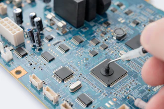
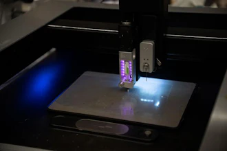
 Process control monitors include optical metrology at Promex using a Nikon INEXIV vision measurement system. At the tolerances required by today's sensor-integrated medical devices, measurement is not a final inspection step — it is an integral part of the manufacturing process itself.Promex
Looking Ahead
Sensor innovation will continue to accelerate. New MEMS architectures, optical technologies, biochemical sensing platforms, and integrated diagnostic systems will enable increasingly sophisticated medical devices.
At the same time, manufacturing will play an increasingly important role in determining which technologies successfully reach patients and healthcare providers.
The next generation of sensor-driven devices will not be defined solely by sensor sensitivity. They will be defined by how effectively engineering teams can integrate materials, assembly processes, metrology, and manufacturing workflows into a scalable system.
For today's medical device designers, that means viewing manufacturing not as the final step in development, but as a fundamental component of sensor performance itself.
Justin Weltmer is a senior process engineer at Promex Industries specializing in advanced microelectronics assembly, heterogeneous integration, and manufacturing process development for highly complex devices. He has experience supporting medical device, biotechnology, aerospace, and defense programs, with expertise spanning materials selection, flip chip assembly, advanced packaging, and design-for-manufacturability. Justin works closely with engineering teams to develop robust manufacturing processes that improve reliability, yield, and scalability from prototype through production. Promex Industries provides advanced microelectronics assembly and manufacturing services for medical, biotechnology, and high-reliability applications.